|
|
8-Bit Analog to Digital Converter Module
with Window Comparator Option
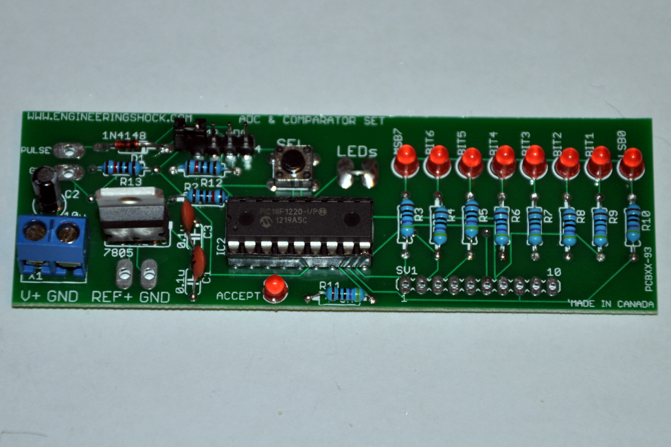
This listing is for an 8-bit analog to digital converter module that is fully assembled and tested. We also sell these in DIY kit form for a few dollars less. Below there is a demonstration video that shows you each of the operations that this device has to offer. There are two header connectors labelled "ADC" & "COMP". We will talk about these later. The ADC can read any voltage between 0-5v. Any voltage higher than that will harm the chip, so be very careful not to exceed 5v. This module requires 7-12v to operate. There is an on-board 5v regulator. There is also a power saving option. If you don't short the two "LEDs" pins together, the LEDs will not operate. If you short this connection, the LEDs will share a common path to the ground line, which will allow for them to emit light. If you don't want to see the logic on the LEDs, then don't short these two pins. By default, this module comes with these lines shorted. There are three settings that this module offers:
1) Free Running Mode: This is the default operation of this module. The ADC samples the input voltage and outputs the 8-bit information several times a second. This logic is displayed for you on eight on board LEDs and can be seen on the 8 outputs lines. In this mode, the ADC is always sampling, and outputting constantly. To Achieve this mode, power the device on with no connections made to the COMP or ADC headers. Leave them unconnected. Watch the demonstration video for reference.
2) Custom Sample Mode: To achieve this operation, place your two pin header connector on the ADC header. When you short these two pins, and power on the device, you will enter into "Custom Sample Mode". The mode cannot be changed on the fly. You have to have your header present on power up. In this mode, the ADC will only sample when you press the SEL button, or when you add an external digital 5v pulse from the "PULSE" input. The pulse input can be soldered to and interfaced with an external digital circuit. Watch the demonstration video for reference.
3) Window Comparator Mode: To achieve this operation, place your two pin header connector on the COMP header. When you short these two pins, and power on the device, you will enter into "Window Comparator Mode". The mode cannot be changed on the fly. You have to have your header present on power up. In this mode, you set the upper threshold voltage (As seen in the video) and the lower threshold value by pressing the SEL buttons. When you program the high and low threshold voltage, the "ACCEPT" LED will flicker. After you program in these voltage, you are ready to roll. When the voltage on the REF+ pin is higher than the high input voltage threshold, the BIT2 LED will light up. When the voltage is within the window (In between the high and low voltage thresholds) the BIT1 LED will light up. When the voltage at the REF+ pin is lower than the low voltage threshold that you've programmed, the BIT0 LED with light up. It really is better if you watch the demonstration video.
Specification:
Input Voltage: 7 - 12VDC.
Size: 10cm(L) x 3.3cm(W) x 2.3cm(H)
Pins and I/O Information:
V+: This is your input voltage pin. Place 7-12v here.
GND: There are four pins on the board that have a direct ground connection. All are labelled except for one on the output chain.
REF+: This is your ADC sampling pin. Make sure not to place more than 5VDC on this line, or you can damage the programmed IC.
PULSE: When in Custom Sample Mode, you can use the button on the board to sample the REF+ line, or you can externally send a 5v pulse to this line, which will tell the chip to sample the REF+ line.
LEDs: These two pins must be shorted together for the LEDs to work properly. If you sever this connection, the LEDs will not operate. This is a power saving mode.
Pin#10: Regulated 5v for external powering (Can supply 600mA)
Pin#9: This is a ground pin. You can use this to interface with an external circuit.
Pin#8: This is the BIT0 LSB (Least Significant Bit) Output, which corresponds to the LSB0 LED (Binary Value = 1)
Pin#7: This is the BIT1 output that corresponds to the BIT1 LED (Binary Value = 2)
Pin#6: This is the BIT2 output that corresponds to the BIT2 LED (Binary Value = 4)
Pin#5: This is the BIT3 output that corresponds to the BIT3 LED (Binary Value = 8)
Pin#4: This is the BIT4 output that corresponds to the BIT4 LED (Binary Value = 16)
Pin#3: This is the BIT5 output that corresponds to the BIT5 LED (Binary Value = 32)
Pin#2: This is the BIT6 output that corresponds to the BIT6 LED (Binary Value = 64)
Pin#1: This is the BIT7 MSB (Most significant Bit) output, which corresponds to the MSB7 LED (Binary Value = 128)
The Schematic Can Be Found Here: http://www.electroniclessons.com/adc.pdf