|
|
|
|
|
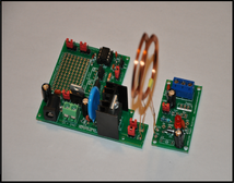
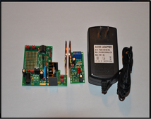
The wireless power transfer kit version#1 - Comes with TX & RX kit & AC Adapter
ARE YOU LOOKING FOR THIS ITEM, OR ANY ITEM IN BULK? WANT AN AWESOME PRICE? JUST ASK!
This listing is for a new wireless power transfer DIY electronics kit. This is the version#1 kit that includes a 12v 2A AC Adapter, as well as the transmitter and receiver kits. This listing does not include the switch, booster, or LED bank. The version#2 set of this kit can be found below, and includes these items. This kit is sent out in DIY kit form. You put it together yourself based on the detailed assembly video found below. It is relatively easy to put together and test. I can assemble and test it for you for an extra $10, but you need to message me before purchasing. This kit is great for home experimentation, science projects, etc. When you purchase this listing, we can send you the schematic diagrams to the email address associated with your paypal account!
Through the process of inductive coupling, you can literally transfer power from one coil of wire to another. Very much like a transformer. After the transmitter is powered up for about 10 seconds, it will consume about 300-350mA. From there, if the receiver is loaded with a load/circuit, it can draw up to 450mA if the transmitter and receiver coils are in parallel with one another and very close together. The receiver voltage is rectified, and the voltage range depends directly on the proximity of the coils. This voltage should not exceed 8VDC. Boosters are very helpful here, so you might want to have a look at the version#2 linked below.
There is also a prototyping area on the transmitter board. There is a power rail and a ground rail. You can select between the input voltage (12v), or a regulated 5v to be on the power rail of the prototyping area by adjusting the 5V/V+ rail. If you have the jumper selecting 5V, then the power on the voltage rail will be a regulated 5v. If you select V+ on this header, then the voltage on the power rail will be 12v.
These sets were initially designed as a learning aid for myself. I designed these boards to be wireless charger prototyping boards. There are components that are not populated on each board. However, if you wish to do your own prototyping with these boards, you will have access to the schematic diagrams if you purchase this listing. I've set out nominal components for this set. It does not mean that you have to follow exactly what I do. However, I provide a set of components that work well, so that you can easily get started with your wireless power adventure!
Power Options:
Once assembled, you can use the included AC adapter to power this set. However, if you are doing your own modifications to the circuitry provided, it is EXTREMELY important for you to have a bench top power supply, so that you can see how much current is being consumed. If you use other components of your own to experiment/modify this set, then you can cause the transmitter to require way too much current, and this can damage certain components on the board and your AC adapter. If you have a bench top power supply, you can use the terminal block power port to power the device. This is a secondary power input. The V+ terminal is where you place your positive voltage, and the GND terminal is where you connect your power supply ground.
Other Prototyping Options:
I'll mention it now. If you modify this kit at all, and you don't know what you are doing, you can damage it. Please keep in mind that this is a project board. Be careful with it. However, there are some interesting options here that I should mention. You can disable the on-board oscillator by modifying the jumper on the ON/OFF header. You would only do this if you wanted to apply your own digital signal to the FET. If you want to turn off the oscillator, place a jumper on the OFF pins. By default, the oscillator should always be on. A Jumper should be placed on the ON pins of the header. If you have a jumper selecting OFF, you can apply your own signal the the FET by connecting said signal to the INT/EXT header. If you have a header selecting the INT pins, the the signal driving the FET is the internal oscillator. If you have the EXT pins selected, then the signal driving the FET will be the external signal that you provide on the 2-pin EXT-GND header. To connect an external 0-5v signal, connect the signal to the EXT pin, and the signal circuit ground line to the GND pin. There are also several test points that are outlined in the schematic diagrams that you can take advantage of.
When you purchase version#1 (This listing), you will receive the following:
1) 1x Wireless Power Transmitter DIY Kit
2) 1x Wireless Power Receiver DIY Kit
3) 1x 120-240VAC 50/60Hz to 12VDC @ 2A Wall Adapter
4) You can contact me for the schematic diagrams through the link above. I will answer as fast as humanly possible =D
Some Preliminary Things To Note:
1) You need to pay close attention to detail when putting these kits together. Watch the entire assembly/test video before powering up for the first time.
2) The heat-sinked FET and the 100x 0.1uf capacitor will get warm. This is normal. However, if you test, and the receiver board LED does not turn on when the receiver coil is within close proximity of the transmitter coil, then POWER OFF IMMEDIATELY and CAREFULLY check the heat on the heat sink. If it is very hot, then you've got an issue. I can always help to troubleshoot, but this isn't a problem that you should be having if you are extremely careful during assembly. This is why it is so important to watch the assembly/demo video in full. If you run into problems, contact me through the above link.
3) While these kits are not overly difficult to put together, it is good to have someone with experience supervise the assembly. If you don't have any experience with kit making, then please ensure that you are working with someone who does. You will find that this will be very helpful to you.
You can view the Version#2 kits here: Click Here
Questions?
Please do not hesitate to ask. I'll do my best to answer promptly!
Assembly Video: